IT House reported on March 17 that Sony Semiconductor’s official website has now listed the IMX820 full-frame CMOS sensor, which uses a 24-megapixel partially stacked design, but the detailed specifications are not listed in the white paper.
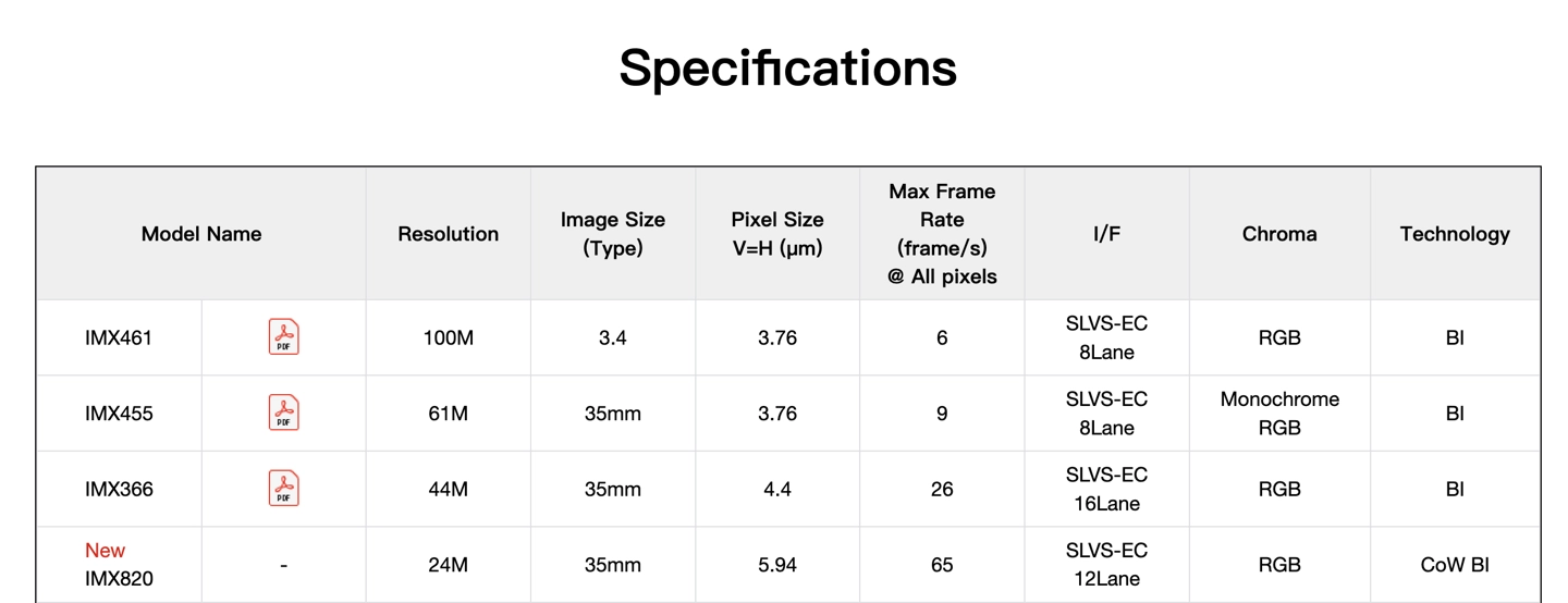
According to source SonyAlpha Rumors the day before yesterday, this sensor is currently used in products such as Nikon Z6III and Panasonic Lumix S1II. However, Soban does not list the 33-megapixel partially stacked sensor on the Alpha 7 V camera. Currently, this CMOS is only used exclusively by Sony, and the benefits do not flow to outsiders.
Sources said that this 33-megapixel partially stacked sensor will be exclusive until 2027. After that, manufacturers such as Nikon are also expected to get the same CMOS.
It is worth noting that the IMX820 sensor is equipped with "CoW BI" technology, so we have reason to speculate that the 33-megapixel CMOS of the Alpha 7 V also uses the same technology.
For reference, semiconductor manufacturers usually use WoW (IT Home Note: Wafer-on-Wafer, wafer to wafer) technology to package CMOS, laminating the entire pixel wafer with the entire logic circuit wafer, and then cutting it into individual sensors.
The CoW (Chip-on-Wafer) technology is different. One of the wafers is first cut into individual chips, and then these independent chips are attached to another entire uncut wafer. This technology can bring many advantages.
One of these advantages is the reduction of silicon wafer waste, because the pixel layer area of the full-frame/medium-frame sensor is very large, and the traditional WoW solution requires that the size of the logic circuit wafer bonded under the pixel wafer exactly matches, resulting in a lot of silicon wafers being wasted. CoW can attach small logic wafers to larger sensors without completely matching the size, greatly improving resource utilization.
Moreover, the yield rate of WoW packaging technology is not high. If the logic wafer is defective, the intact pixel wafer above will be scrapped. CoW, on the other hand, can screen out good-quality wafers before laminating them, significantly improving yield and reducing manufacturing costs.
In addition, CoW technology can also apply microscopic copper-to-copper (Cu-Cu) hybrid bonding technology to attach A/D converters, DRAM, etc. directly on top of the pixel wafer, which can bring higher parallel data processing capabilities and achieve a global shutter without jelly effect.